毕磊
Academic Honor:
2015 国家优秀青年基金获得者
Integrated Photonic Materials and Devices
Integration is the main developing trend of photonic materials and devices. Currently, silicon photonic integrated circuits (PICs) and optical metasurfaces require optical thin films instead of bulky crystals, as well as planar integrated micro and nanophotonic devices instead of discrete components. In the micro and nano scale, new physical phenomena emerge when light and matter interact. The structure and fabrication method of optical thin films diverse from their bulk counterparts; and the device structure and operation principle are vastly different. Our group dedicate in studying the mechanism between light and matter interaction at the nanoscale. We study heterogeneous integration of key optoelectronic and optomagnetic materials on silicon. We also develop heterogeneously integrated silicon PICs and optical metasurfaces with the aim of application in next generation optical communication, data communication and optical sensing microsystems.
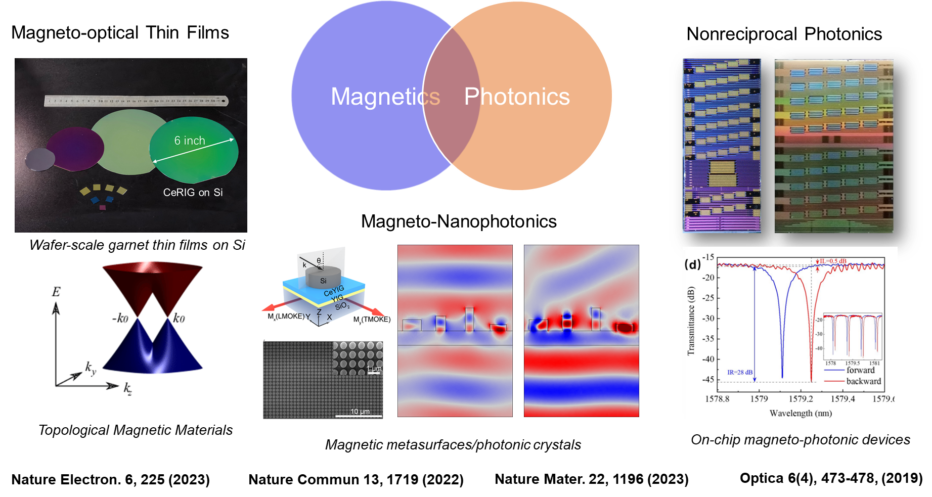
Magneto-optical thin films and integrated nonreciprocal photonic devices
Nonreciprocal photonic materials including optical isolators, circulators and phase shifters based on magneto-optical thin films are key components in photonic systems. They are widely used in optical communication, data communication and optical sensing. However, the principle of nonreciprocity in nanoscale photonic structures is unclear. The technology to integrate magneto-optical thin films and devices on semiconductors is not mature, causing such materials and devices absent in photonic chips, which is called the “fundamental challenge for integrated photonics”.
Our group study the new nonreciprocal photonic mechanism in magnetic nanophotonic structures. We develop heterogeneously integrated magneto-optical thin films on silicon. We develop silicon waveguide integrated nonreciprocal photonic devices. We also study the process integration between nonreciprocal photonic devices and silicon photonic technologies. We aim to apply these materials and devices in optical communication, data communication and optical sensing technologies.
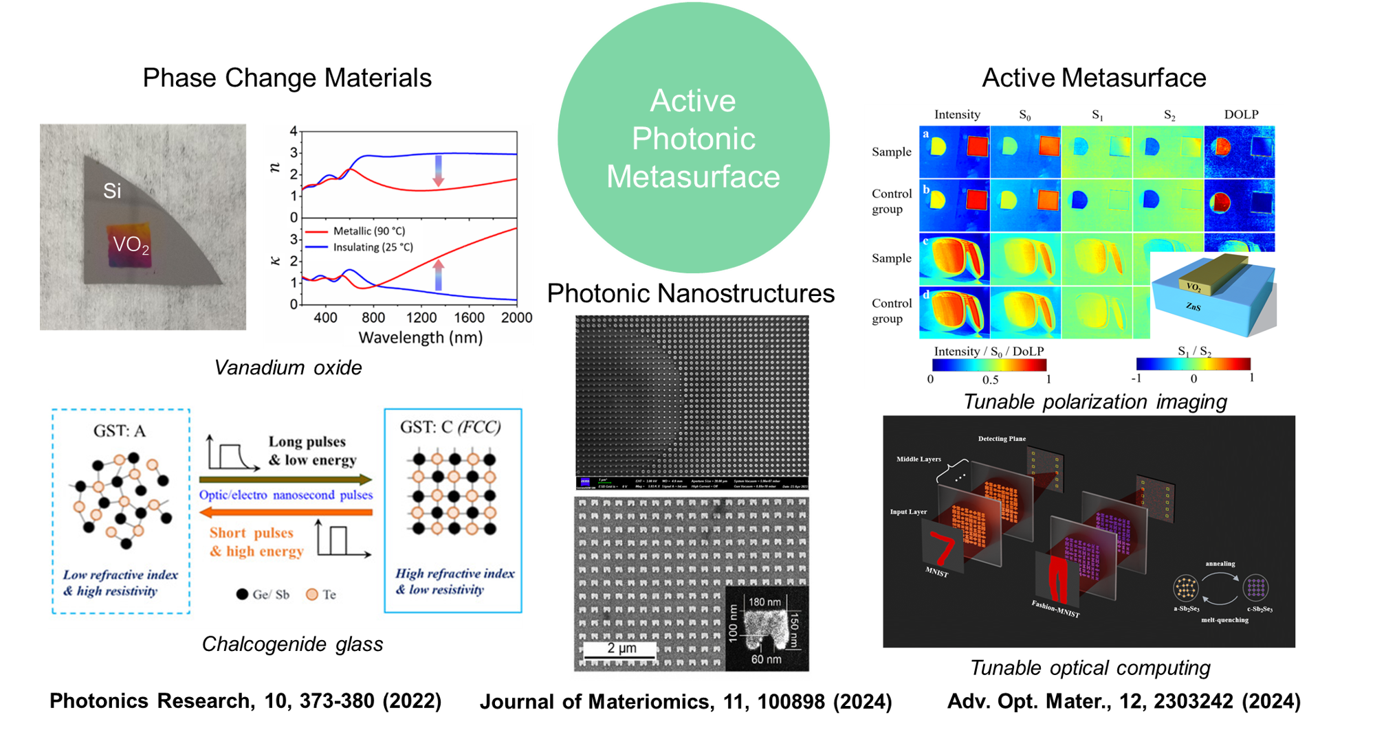
2. Phase change materials and optical metasurfaces
Based on the generalized Snell's law, optical metasurfaces allow planar integration of three dimensional photonic devices, such as prisms and lens, on a two dimensional surface, which is selected as one of the 10 breakthroughs of the year by the journal of Science. The goal for metasurface development is to develop high efficiency, multidimensional and tunable optical metasurfaces for optical imaging, sensing and optical computing applications.
Our group dedicate in studying the light-matter interaction in subwavelength nanostructures of optical metasurfaces. We fabricate photonic nanostructures based on magneto-optical, electro-optical and phase change materials to develop active optical metasurface devices, such as polarization tunable metasurfaces, focus tunable metalens and reconfigurable diffractive metasurfaces. We aim to apply these materials and devices in optical imaging, optical sensing and optical computing technologies.
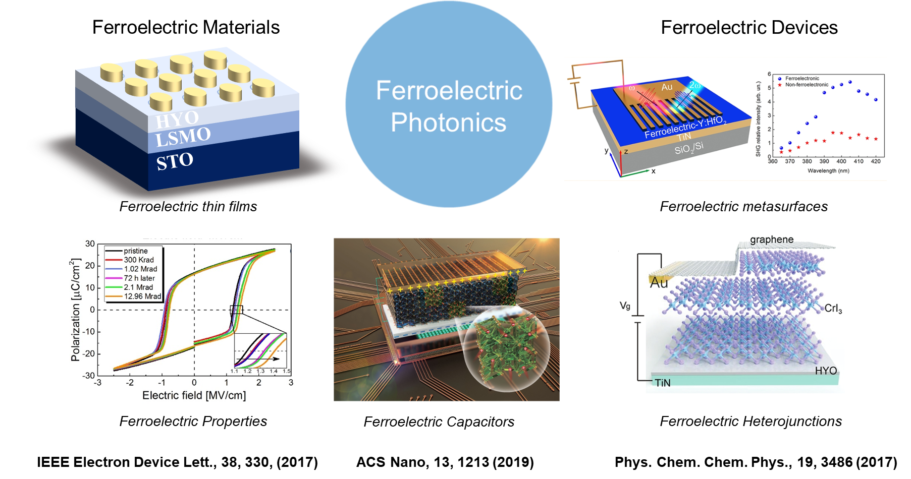
3. Ferroelectric materials and integrated optical modulators
Ferroelectric materials such as LiNbO3, BaTiO3 and HfO2 show electro-optical Pockels effect and nonlinear photonic effect. They are highly desired in next generation optical modulation devices. The goal is to develop high electro-optic coefficient, low loss and silicon photonic process compatible ferroelectric thin films and integrated devices.
Our group dedicate in studying heterogeneously integrated novel ferroelectric thin films on silicon. We develop silicon waveguide integrated optical modulators and nonlinear photonic devices. We aim to apply these materials and devices in optical communication and data communication technologies.
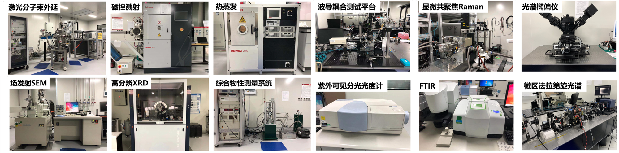
Facilities
Our group share the facilities in National Engineering Center of Electromagnetic Radiation Control Materials, and State Key Lab of Electronic Thin Films and Integrated Devices. Our lab also independently owns research facilities including laser MBE system, sputtering system, e-bema lithography system, optical waveguide characterization system, metasurface characterization system, MOKE/FR characterization system, magneto-optical ellipsometry and semiconductor analysis system etc.